Breaking the Memory Wall: How Ferroelectric Breakthroughs are Reimagining AI Architecture
The current trajectory of artificial intelligence is a race against physics. As large language models and multi-modal neural networks grow in complexity, the primary constraint is no longer just raw computational power—it is the energy and time required to move data between the processor and the memory. This phenomenon, known as the "memory wall," is the single greatest hurdle in the scaling of next-generation AI.
However, a fundamental shift is underway. Recent breakthroughs in ferroelectric memory (FeRAM) are signaling a departure from traditional charge-based storage, offering a path toward more efficient, high-density, and non-volatile computing environments.
The Energy Crisis in Silicon
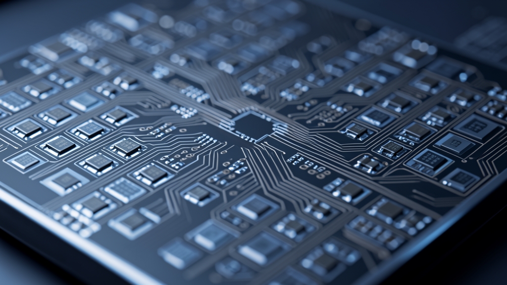
To understand why ferroelectric memory matters, one must first understand the inefficiency of current systems. Most modern computing relies on the Von Neumann architecture, where the Central Processing Unit (CPU) or Graphics Processing Unit (GPU) is physically separated from the memory (DRAM). Every time an AI model performs an inference or a training step, billions of data points must travel across a bus.
This movement is incredibly "expensive" in terms of energy. In many high-performance AI workloads, the energy consumed by moving data back and forth between the memory and the logic unit exceeds the energy used for the actual calculation itself. As we push toward trillion-parameter models, this inefficiency threatens to hit a thermal and economic ceiling.
The Science of Polarization
Ferroelectric memory offers a fundamentally different mechanism for data retention. While traditional DRAM stores information as an electrical charge in a capacitor—which naturally leaks over time and requires constant "refreshing"—ferroelectric memory utilizes the electric polarization of a crystal lattice.
By applying an electric field, the internal dipoles of a ferroelectric material can be switched between two stable states. These states represent the binary '0' and '1'. Because these states are physically stable, the memory is inherently non-volatile; once the data is written, it stays there without requiring constant power.
The recent breakthroughs center on two critical metrics: storage density and switching energy. Historically, ferroelectric materials were difficult to scale down to the nanometer levels required for modern semiconductor fabrication. New advancements in hafnium oxide-based ferroelectrics have solved much of this compatibility issue, allowing these materials to be integrated directly into standard CMOS (Complementary Metal-Oxide-Semiconductor) manufacturing processes.
The Rise of In-Memory Computing (IMC)
The most profound implication of these advances is the enabling of In-Memory Computing. If the memory itself possesses the physical properties required to perform logic operations, the need to move data to a separate processor diminishes significantly.
By integrating ferroelectric layers directly into the logic circuitry, engineers can create "computational memory." In this paradigm:
* Data movement is minimized: Calculations happen where the data lives.
* Latency is slashed: The delay caused by the memory bus is virtually eliminated.
* Power efficiency skyrockets: The energy required to toggle a ferroelectric state is orders of magnitude lower than the energy required to charge and discharge a traditional capacitor.
For edge AI—such as autonomous drones, wearable medical devices, and sophisticated IoT sensors—this is a game-changer. These devices require high-level intelligence but operate under strict battery constraints. Ferroelectric memory provides the "intelligence density" needed to run complex models locally without draining the power source.
Scaling for the Data Center
While the benefits for edge computing are clear, the impact on the data center is perhaps even more transformative. As hyperscalers race to build massive AI clusters, the cooling and power infrastructure required to support them is becoming a logistical nightmare.
High-density ferroelectric memory could allow for much larger models to reside entirely within high-speed, near-compute memory tiers. This would reduce the reliance on massive, power-hungry DRAM arrays and provide a more sustainable pathway for scaling the computational capacity of the global cloud.
The Road Ahead: Manufacturing and Reliability
Despite the technical optimism, challenges remain. Integrating new materials into a mature semiconductor supply chain is a Herculean task. Ensuring the long-term reliability and endurance of ferroelectric layers—essentially how many billions of times they can be switched before the material degrades—is a primary focus for current research.
Furthermore, the industry must standardize how these new memory cells interface with existing software stacks. Transitioning from a world of "compute-centric" design to "memory-centric" design requires a fundamental rethinking of how compilers and operating systems manage data.
We are witnessing the early stages of a hardware renaissance. As the industry moves past the limitations of charge-based storage, the ferroelectric breakthrough may well be remembered as the catalyst that allowed AI to move from massive, energy-hungry server farms into the very fabric of our daily technology.