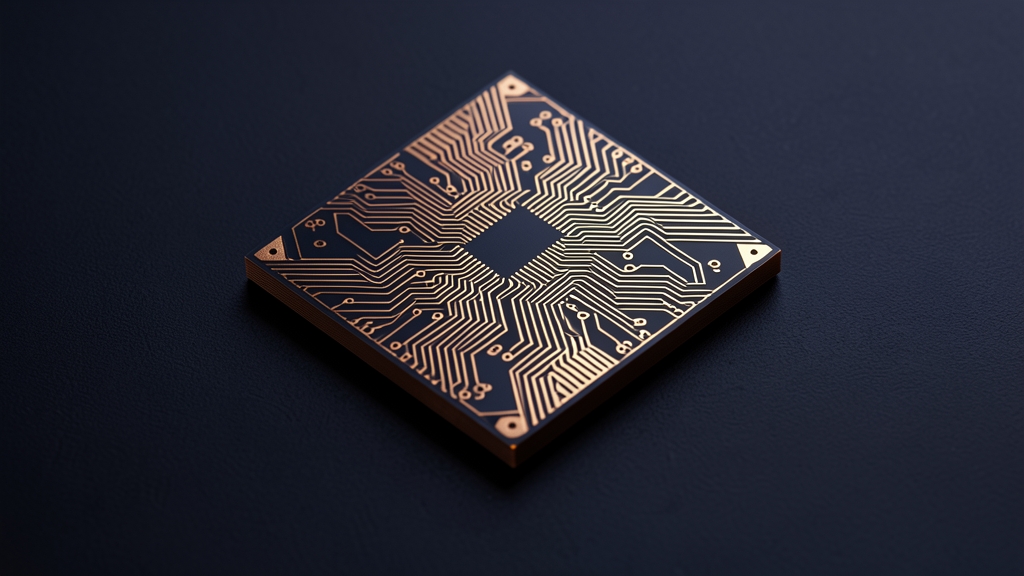
The current landscape of artificial intelligence is defined by a brutal, high-stakes war of attrition over compute. For years, the industry has relied on a standard playbook: build larger models, aggregate more H100s, and hope that the sheer scale of raw processing power can overcome the limitations of existing hardware. But Google is preparing to change the rules of engagement entirely.
Leaked reports and industry intelligence suggest that Google is pivoting away from its existing Tensor Processing Units (TPUs)—which, while powerful, are still fundamentally general-purpose AI accelerators—toward a new class of Application-Specific Integrated Circuits (ASICs). This new silicon isn't just designed to run AI; it is being engineered to bake the specific mathematical architecture of the Gemini model directly into the physical circuitry.
The Architecture-Silicon Marriage
To understand the magnitude of this shift, one must understand the "memory wall" and the bottleneck of data movement. In traditional computing, moving data between a processor and memory consumes significantly more energy and time than the actual computation itself. Even with current high-end GPUs, much of the computational cycle is wasted on the overhead of managing how data flows through the system.
By designing a chip that mirrors the specific transformer-based architecture of Gemini, Google is attempting to achieve what engineers call "architectural-silicon synergy." Instead of teaching a general-purpose chip how to handle Gemini’s specific attention mechanisms and multi-modal processing through software instructions, Google is hardwiring those instructions into the silicon itself.
This move targets the very core of the inference process. When a user asks Gemini a question, the chip won't need to "interpret" how to execute the math; the paths through the transistors are already laid out to match the model’s neural pathways. The projected result is a massive 6–10x gain in efficiency—a number that would fundamentally rewrite the economics of large language models (LLMs).
Breaking the Efficiency Barrier
The implications of a 6–10x efficiency gain cannot be overstated. In the current AI economy, the primary constraint is not just "intelligence," but the cost and power required to deliver that intelligence at scale.
* Latency Reduction: Hardwired logic allows for near-instantaneous execution of complex tensor operations, bringing real-time, multi-modal AI closer to a seamless human experience.
* Power Management: A massive chunk of data center energy is spent on data movement. By optimizing the physical layout for Gemini’s specific weights and biases, Google could drastically lower the wattage required per token generated.
* The Inference Economy: If Google can reduce the cost of running Gemini by an order of magnitude, they move from a position of defending their market share to aggressively undercutting every competitor in the space.
The "Apple-ification" of AI
This strategy represents the ultimate expression of vertical integration. Much like Apple revolutionized the laptop market by designing both the silicon (M-series) and the operating system (macOS) to work in lockstep, Google is attempting to do the same for the AI era.
While NVIDIA remains the undisputed king of the training market, providing the raw brute force required to build models, Google is positioning itself to own the inference market—the phase where models are actually used by billions of people. If Google can control the model, the software ecosystem, and the physical silicon it runs on, they create a closed loop of optimization that is incredibly difficult for competitors to penetrate.
This shift has already sent ripples through the financial markets. Investors are increasingly looking past the "model wars" and focusing on the "compute efficiency wars." The capital is moving toward companies that demonstrate a path to sustainable, low-cost scaling.
The Risk of Architectural Rigidity
However, this "all-in" bet on Gemini comes with a significant technical risk: rigidity.
The field of AI research moves at a breakneck pace. New architectures—such as State Space Models (SSMs) or new variations of attention mechanisms—could emerge that make the current transformer-based design of Gemini obsolete. If Google spends billions of dollars perfecting silicon that is hardwired for a specific mathematical structure, they risk being left with a massive graveyard of specialized, yet useless, hardware if the "next big thing" in AI architecture shifts the goalposts.
General-purpose chips like NVIDIA’s are resilient because they can adapt to any model through software updates. Google’s new chip, by definition, sacrifices that flexibility for sheer, unadulterated performance.
The New Battlefield
As the industry watches, the central question is no longer just "which model is smarter?" Instead, the question has become: "who can run the smartest model the most efficiently?"
Google’s move suggests that the era of general-purpose AI hardware may be entering its twilight. If they succeed, the path to true artificial general intelligence (AGI) may not be paved with more massive clusters of general chips, but with highly specialized, deeply integrated silicon that knows exactly how to "think" before the first electron even moves.