The Silicon Pivot: Inside Google’s Move to Build a Gemini-Native AI Chip
The era of "one-size-fits-all" computing is reaching a breaking point. As large language models (LLMs) evolve from simple text predictors into massive, multimodal reasoning engines, the hardware currently powering them is struggling to keep pace. The bottleneck is no longer just raw compute power; it is efficiency.
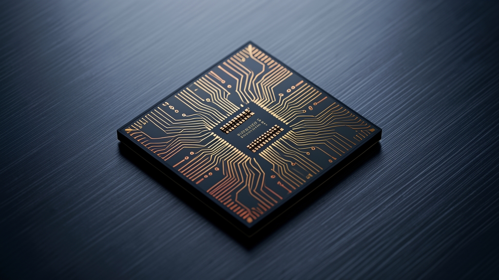
According to reports circulating through the industry, Alphabet is doubling down on its vertical integration strategy. The tech giant is currently developing a new class of custom silicon specifically engineered to run its Gemini models. This is not merely an incremental update to existing Tensor Processing Units (TPUs); it is a fundamental reimagining of how AI hardware and AI software interface.
Breaking the Inference Bottleneck
To understand why Google is making this move, one must understand the "Inference Crisis." While much of the public discourse surrounding AI focuses on the massive compute required to train models, the real economic battle is being fought during inference—the stage where the model actually answers a user's prompt.
Inference is where the margins are won or lost. As Gemini scales to handle longer context windows, high-resolution video, and real-time voice interactions, the computational cost per query scales aggressively. Currently, much of this workload relies on highly capable, but incredibly expensive, general-purpose GPUs. While these chips are masterpieces of engineering, they are designed to be versatile. They are built to handle everything from physics simulations to gaming to training.
A chip designed specifically for Gemini, however, can afford to be a specialist. By stripping away the logic required for non-AI tasks, Google can reallocate that transistor budget toward specific operations that Gemini performs billions of times a day: attention mechanisms, matrix multiplications, and high-speed memory management.
The Architecture of Efficiency: Beyond the TPU
While Google has long been a leader in custom AI silicon via its TPU lineage, the reported new chip suggests a shift toward "model-aware" architecture. This concept, often referred to as hardware-software co-design, involves designing the silicon specifically around the mathematical structure of a particular model family.
Industry analysts suggest that the new hardware likely focuses on three critical technical pillars:
* Memory Bandwidth Optimization: Modern LLMs are notoriously "memory-bound." The speed at which data moves from memory to the processor is often a bigger bottleneck than the processor's speed itself. A Gemini-native chip may utilize advanced packaging techniques or specialized high-bandwidth memory (HBM) configurations to ensure the model's massive parameters are fed to the compute cores without delay.
* Sparsity and Quantization Logic: Not every "neuron" in a model needs to fire for every prompt. Specialized hardware can exploit "sparsity"—skipping the calculations for zero-value weights—to save massive amounts of energy. Furthermore, by building hardware that natively supports lower-precision math (such as FP8 or even INT4), Google can run more complex models using a fraction of the power.
* Multimodal Acceleration: Gemini is designed to be natively multimodal. This means it doesn't just process text; it understands images, audio, and video as primary inputs. A dedicated chip can include specialized "engines" for vision processing and audio signal transformation, preventing the core logic from being overwhelmed by non-textual data streams.
The War for Vertical Integration
Google’s move is a tactical strike in a larger geopolitical and economic war. For much of the last few years, the AI industry has been defined by its dependence on a single source of compute. This "Nvidia Tax"—the high premium paid for cutting-edge GPU access—has become a significant drag on the balance sheets of every major AI player.
By moving toward a custom, Gemini-centric silicon stack, Google is attempting to build a moat that is both technical and economic. If Google can run Gemini more cheaply and faster than its competitors can run their models on third-party hardware, it gains an insurmountable advantage in the race to provide ubiquitous, low-latency AI services.
This is the same playbook utilized by Apple. By controlling both the silicon and the software, Apple ensures that its devices provide a seamless, highly optimized experience that is difficult for competitors to replicate using off-the-shelf components. Google is now applying this logic to the data center.
The High-Stakes Challenge
However, the path to silicon sovereignty is fraught with risk. Designing custom chips is an incredibly capital-intensive endeavor with long development cycles. There is also the "software trap": a chip is only as good as the compilers and frameworks that allow developers to use it. Google must ensure that its software stack remains flexible enough to accommodate future iterations of Gemini, even as the hardware becomes more specialized.
Furthermore, the industry is moving at a blistering pace. A chip designed today for the specific requirements of current Gemini architectures must still be robust enough to handle the next leap in model intelligence.
As the lines between software and hardware continue to blur, Google's latest venture signals a clear reality: in the future of artificial intelligence, the winners won't just write the best code—they will build the machines that breathe life into it.