===The End of the Shrinking Era===
For decades, the semiconductor industry has operated under a singular, almost religious mandate: shrink the transistor. This relentless pursuit, governed by the principles of Moore’s Law, has driven the digital revolution, allowing engineers to pack billions of microscopic switches onto a single sliver of silicon. But the industry is currently colliding with a brutal reality. We are approaching the atomic limit.
As transistors shrink toward the scale of a few nanometers, the physics of silicon begins to fail. Electrons, which should stay confined within their designated channels, begin to "leak" through barriers due to a phenomenon known as quantum tunneling. This leakage generates immense heat and renders traditional scaling inefficient, if not entirely impossible. The industry has spent years searching for a way to continue increasing density without succumbing to the heat death of the chip.
Enter IBM. While the tech giant has long retreated from the high-capital, low-margin world of semiconductor fabrication—leaving the heavy lifting of chip-making to titans like TSMC and Samsung—it has just executed a move that may be more impactful than building a factory. IBM is not becoming a chipmaker, but it has just provided the blueprint for what comes after silicon.
===The Breakthrough: Atomic-Scale Heterostructures===
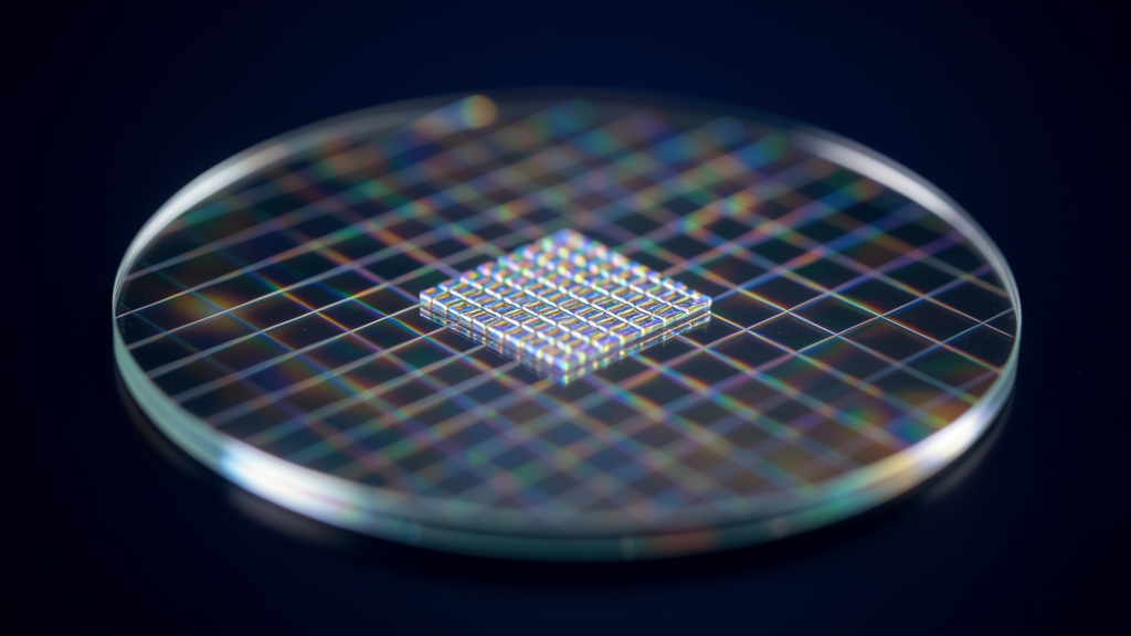
The revolution lies not in how we arrange silicon, but in what we use instead of it. IBM’s research teams have successfully demonstrated a method for engineering "heterostructures" using two-dimensional (2D) materials.
Unlike silicon, which is a bulk material, 2D materials—such as molybdenum disulfide or graphene—are only one or a few atoms thick. These materials possess extraordinary electronic properties, including higher electron mobility and better thermal management, which are essential for the next generation of high-performance computing.
The technical hurdle has always been integration. How do you take these delicate, atom-thin layers and integrate them into a functional, scalable architecture? IBM’s breakthrough involves a proprietary method of "atomic-scale precision engineering." By precisely stacking these different 2D layers, they can create a customized electronic environment. This allows for the creation of transistors that are not only smaller than the current silicon limit but are also significantly more efficient at controlling electron flow.
Key technical advantages include:
* Suppression of Quantum Tunneling: The unique bandgap properties of these 2D materials allow for tighter control over electrons, virtually eliminating the leakage that plagues sub-3nm silicon chips.
* Superior Thermal Conductivity: The materials used in these heterostructures dissipate heat more effectively, solving one of the primary bottlenecks in modern data center scaling.
* Vertical Scaling (3D Integration): Because these materials are atomically thin, they open the door to much more efficient 3D stacking, allowing for increased computational density without the massive power draw.
===A Shift in the Power Dynamics===
This move represents a profound strategic pivot. By focusing on material science and IP (Intellectual Property) rather than the massive capital expenditure required for a new fabrication plant (a "fab"), IBM is positioning itself as the ultimate gatekeeper of the post-silicon era.
In the current landscape, the value is split between the architects (Nvidia, Apple) and the builders (TSMC, Intel). IBM is carving out a third, more foundational tier: the material providers. If the industry's future depends on these 2D heterostructures, every major foundry and designer will eventually need to license the architectural blueprints and material processes developed by IBM.
"We are seeing a transition from an era of geometric scaling to an era of material scaling," says one industry analyst. "In the past, you won by being able to draw smaller lines. In the future, you win by knowing which atoms to stack in what order."
===Market Impact: AI and the Quantum Imperative===
The timing of this breakthrough is critical. The global explosion of Generative AI has created an insatiable demand for compute power. Current GPU architectures are hitting power density walls; the more AI models grow, the more energy they require, and the more heat they generate. The ability to deploy 2D-material-based chips could provide the efficiency leap required to make massive-scale AI sustainable.
Furthermore, this research feeds directly into IBM's long-term quantum computing roadmap. Quantum processors require extreme precision and minimal environmental interference—requirements that silicon-based architectures struggle to meet at scale. The ability to engineer materials at the atomic level is a prerequisite for the stable, fault-tolerant quantum computers of the future.
===The Road Ahead===
Despite the excitement, the path to commercialization is fraught with challenges. Transitioning from a controlled laboratory environment to a high-volume manufacturing line is a monumental task. Foundries like TSMC will need to retool their entire processes to accommodate these new materials, a shift that could take years and billions of dollars.
However, the message from IBM is clear: the silicon era is hitting its ceiling, and the industry cannot afford to stop moving upward. By mastering the atom, IBM has ensured that while they may not be printing the chips, they will be defining exactly what those chips are made of.